Expansion interfaces
This section describes the Grove, MikroBUS and Arduino R3 expansion interfaces:
MikroBUS sockets
![]()
Socket introduction
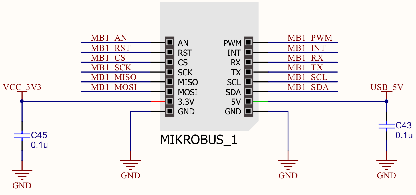
The mikroBUS™ socket comprises a pair of 1×8 female headers with a proprietary pin configuration and silkscreen markings. The pinout consists of three groups of communications pins (SPI, UART and I2C), six additional pins (PWM, Interrupt, Analog input, Reset and Chip select), and two power groups (+3.3V and 5V).
The company Mikroelectronica produces over 500 expansion boards called "Click modules", available through various distributors. These modules are often useful for rapid prototyping and evaluation of a broad variety of sensors, interfaces and actuators.
The figure below shows the MikroBUS#1 schematic, the second interface is identical.
Pinout
The pin-mapping to the MCU is listed in the pinout section. The pinout table shows also the alternative functions when available (as a CAN Bus or I2S interface for audio for instance).
Pin sharing limitation
Please note that, although the STM32F413 MCU provides a rich set and number of peripherals, in some cases the buses need to be shared between the expansion interfaces.
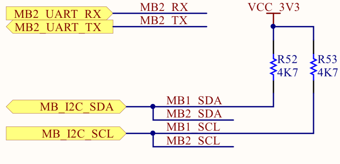
For example, both MikroBUS sockets share one SPI bus, which doesn't present a problem if this interface is used as a bus, since each interface has it's own Chip Select line exposed (MBx_CS), but if these pins are intended to be used as independent GPIOs, only one interface can be used at a time. Refer to the Pinouts section for more details.
The capture below shows the I2C pull-up resistors. Note the I2C lines shared between the MikroBUS 1 and 2 interfaces:
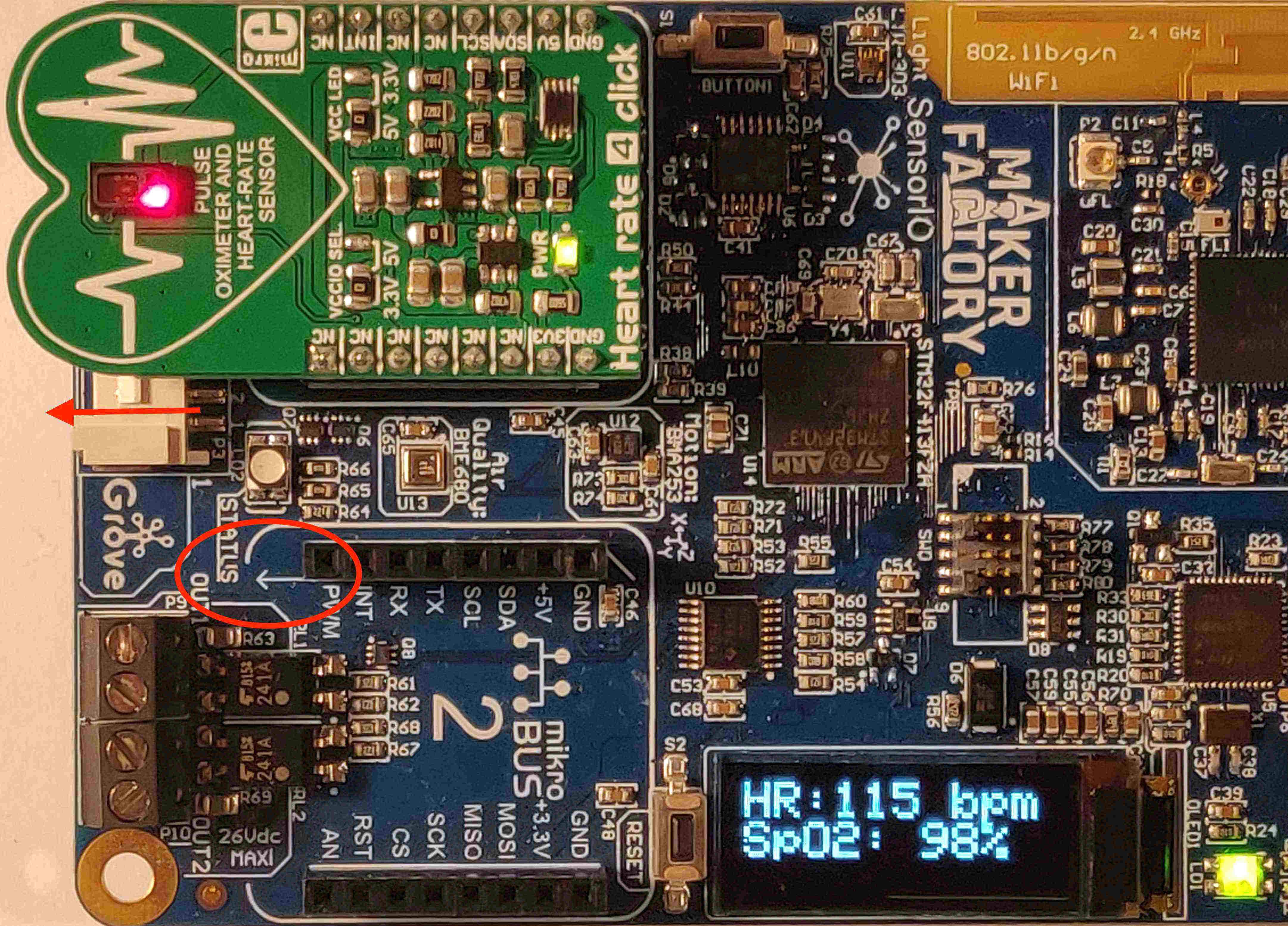
Click boards orientation
Please note the correct orientation mark in the image below. An incorrect installation could damage the module or the SensorIO board.
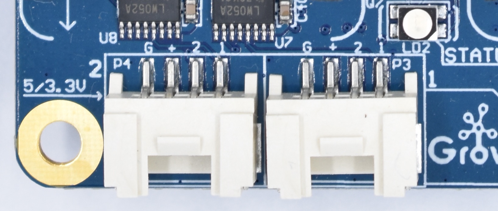
Grove connectors
![]()
Grove system introduction
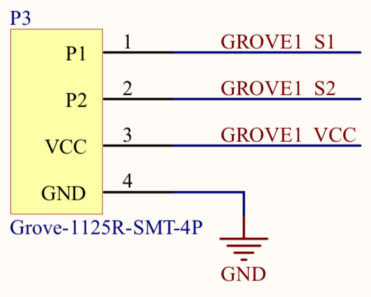
The Seedstudio’s Grove system consist of a 4-pin standardized connector and expansion boards that are attached using extension cables.
The connector uses two pins for power (GND and 3.3V or 5V depending on the module) and two for signals:
Grove interface types
There are basically 4 types of interfaces for these modules:
- Digital: both pins are either digital Input or Output. Usually used for relays or motor control, but some modules also use proprietary control protocols as in the LED Bar module.
- Analog: 2 analog inputs. Common modules providing analog levels are potentiometers and gas sensors.
- UART: Full-duplex serial interface (TXD and RXD). The RF Link module or RFID reader use this interface for instance.
- I2C: This bus can support daisy chaining in some cases. Some sensor modules and LCD displays use this bus.
The image below shows the Grove connectors marking and the corresponding signal names.
Analog multiplexers
As each pin can be used to connect up to 4 different types of peripherals (PWM / I2C / UART and Analog input) and these peripherals in most cases aren't mapped to the same pins on the MCU, each connector is routed through a 2-channel 4x1 Analog Multiplexer SN74LV4052A.
The figure below shows the internal logic of the MUX:
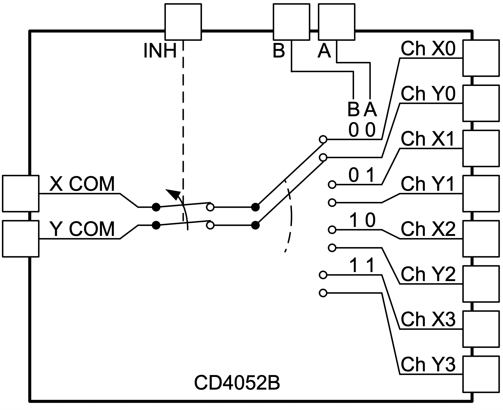
X and Y are the two selectable channels (they can be viewed as switches with 4 positions). The switches position is controlled by the digital inputs A and B (INH disable the switches and it's not used). Therefore the connection from X to (X0 .. X3) depends on the state of the control inputs [B:A].
The schematic below shows the multiplexer for the Grove 2 connector (Grove 1 follows the same schema):
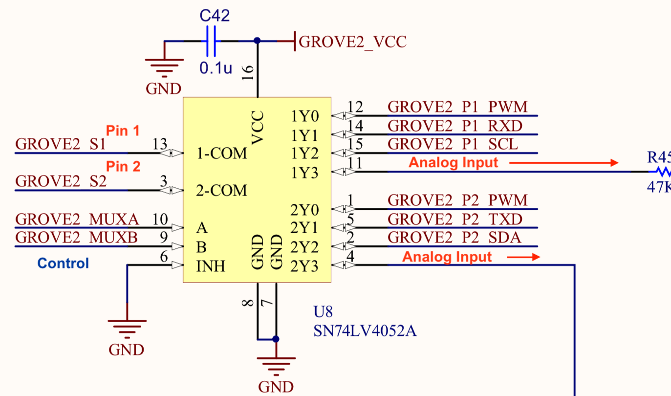 On the left side are routed the pin 1 and 2 of the connector and the control pins and on the right-side the peripherals to the MCU. The analog input is routed to the level conditioning stage detailed below.
The following table shows the configuration for the control pins of the multiplexers (logic levels for A and B). The pin mapping for each connector and the corresponding multiplexed peripherals can be found on the pinouts section.
| Position | Grove_n_MUX_B | Grove_n_MUX_A | Peripheral Connected |
|---|---|---|---|
| 0 | 0 | 0 | PWM (default) |
| 1 | 0 | 1 | UART |
| 2 | 1 | 0 | I2C |
| 3 | 1 | 1 | Analog In |
Level conditioning
Analog levels conditioning
Some Grove modules are designed to work with 5V supply and they provide a 0 to 5V analog output. As the maximum input voltage for the MCU's integrated ADC is 3.3V, a level conditioning and protection stage is added per channel (replicated 4 times).
The image below shows the circuit for the pin 1 of the Grove 2 connector. R45 and R46 transtlate the input voltage with a ratio of 0.68. The operational amplifier U6C acts as a buffer to provide better input impedance to the ADC channel. The input impedance presented to the Grove pins is then 147 kΩ.
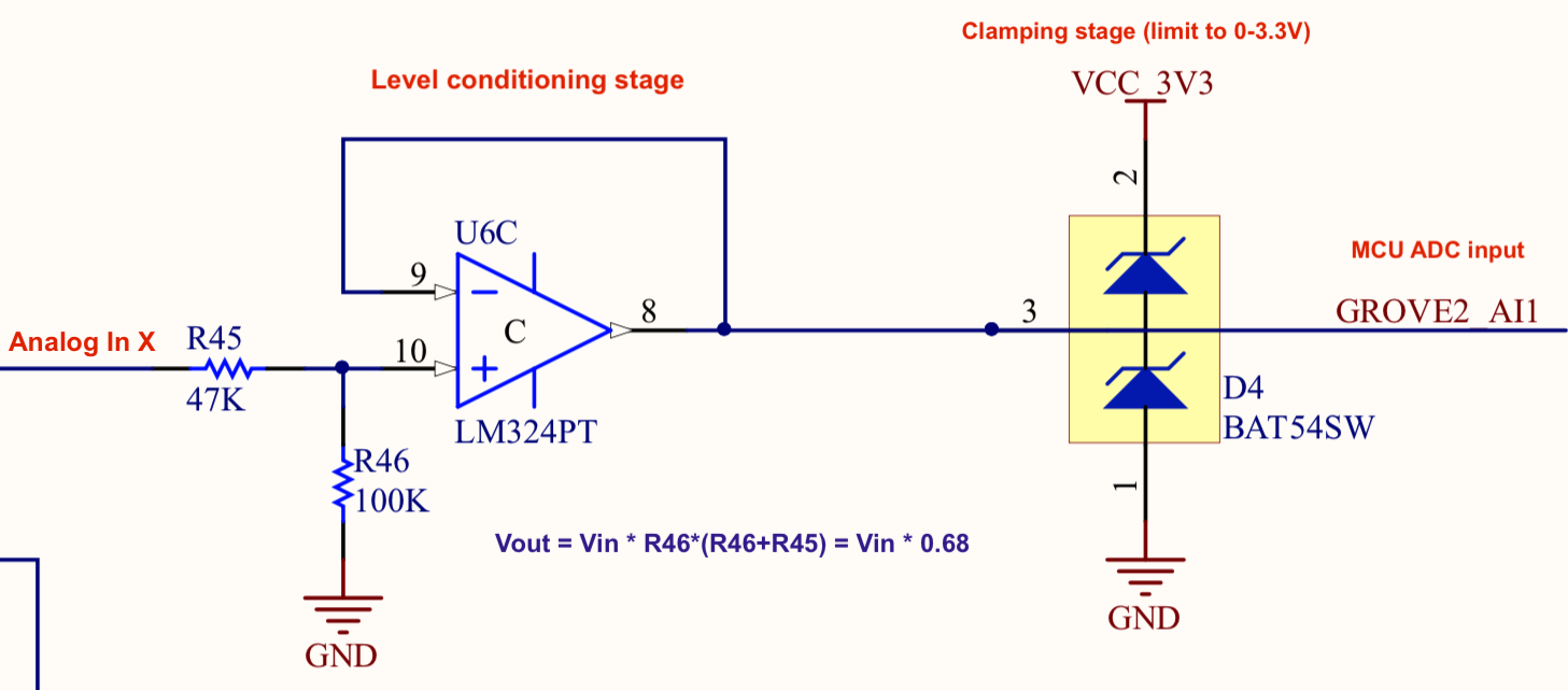 The double Schottky diode D4 limits the voltage at the ADC input to approximately -0.3V or 3.6V to protect the MCU in case that the input voltage exceeds the allowed limits.
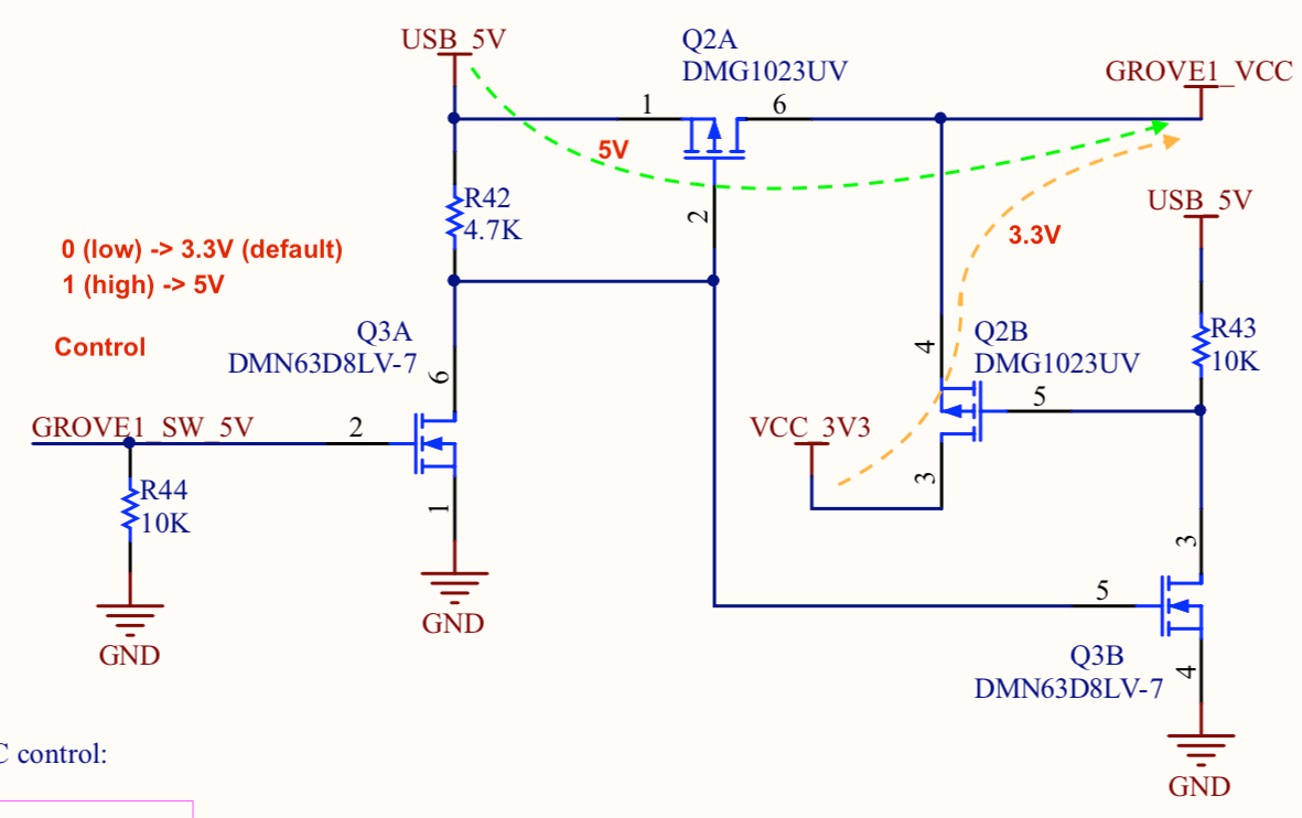
Power switches
Software configurable 5V / 3.3V power switches
As some of the Grove modules support either 5V or 3.3V power only, SensorIO integrates two separate software-configurable 5/3.3V switches to provide the proper voltage to the power pins. Most boards support only 3.3V for the interfaces and power, and some of them provide the option to switch to 5V by unsoldering/soldering resistors or manually changing the position of jumpers. SensorIO has a software-controlled switching functionality, individually per connector for maximum flexibility.
The schematic below shows the power switch for the Grove 1 connector. When the control pin is low (default), the output will provide 3.3V, when the output is pushed high, the power pin will be connected to 5V.
Arduino R3 socket
The Arduino R3 socket is a traditional form factor and there are multiple companies providing extension boards or so called "shields" for different applications. The figure below shows the pinout:
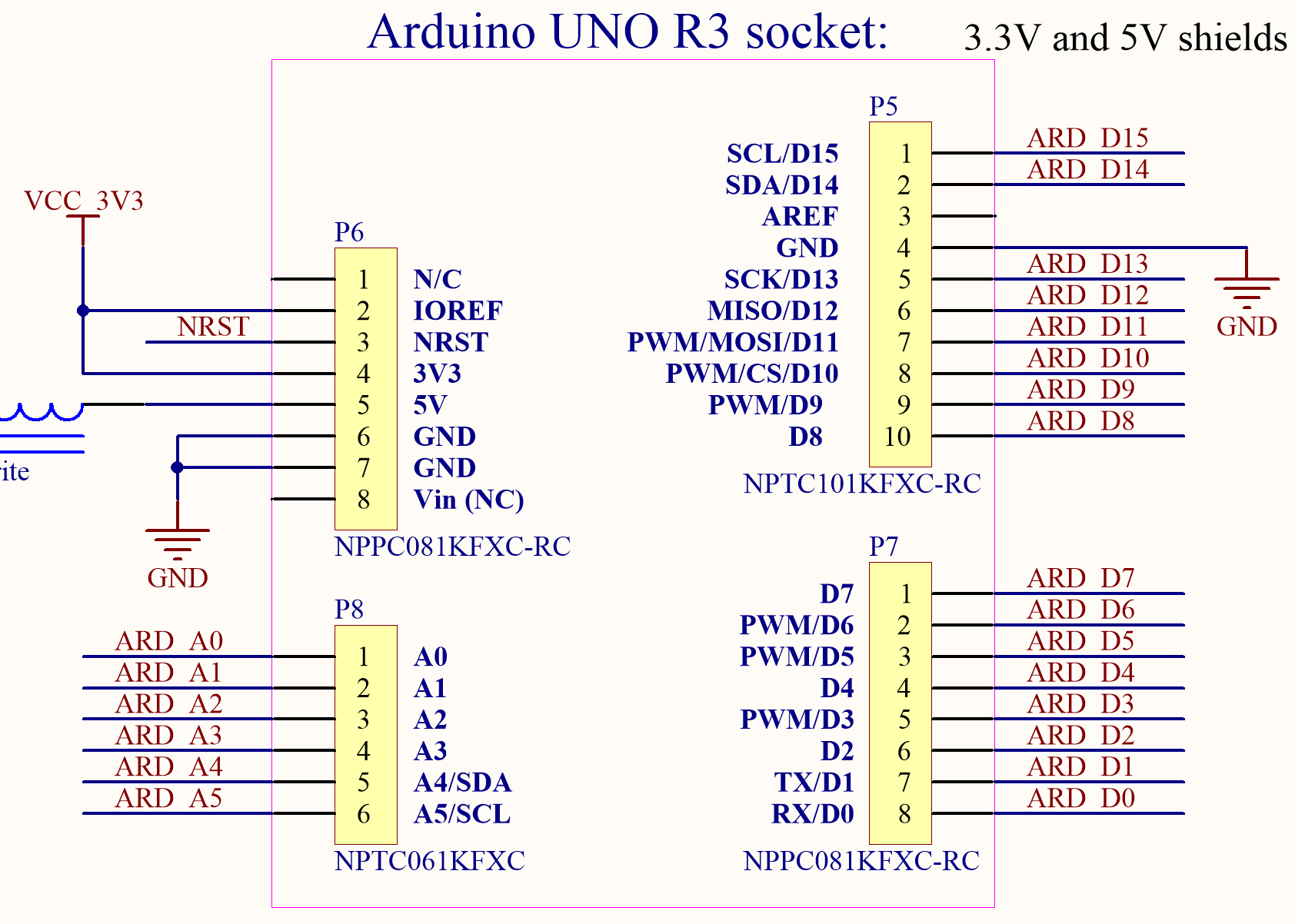
The NRST input signal is connected to the reset line driven by the main Reset push-button (S2). Some shields use this signal to initialize their internal logic (as is the case of some GPS / GSM modem shields).
The IOREF pin is optionally used by some shields to select the digital pins interfacing level (3.3V or 5V).
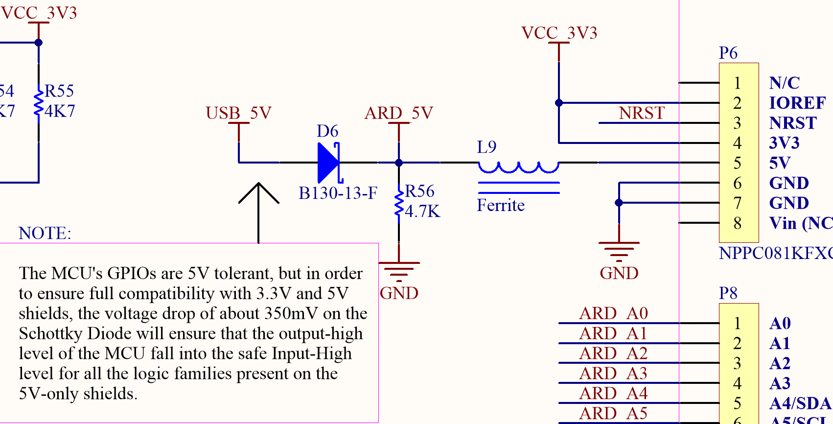
5V compatibility for inputs and outputs
Some Arduino shields use 5V logic levels for the digital interfaces. This doesn't present a problem for the STM32F413 inputs since they are 5V tolerant. The issue would be evident when the MCU outputs are used to drive the inputs on these shields: some logic families are compatible with 3.3V input levels, but some are not. To overcome this potential incompatibility, the board uses a Schottky diode (D6 in the capture below) in series with the 5V power rail to produce a small voltage drop on the Arduino 5V pin. This reduces the shield Vcc to about 4.7V, which is not an issue for the correct functioning of these logic families since it's tolerated in the nominal range, but enough to allow the outputs of the MCU to fit in the safe range for the logic HIGH (in other words: a 3.3V output on the MCU will ensure a high level on the shield's inputs for all the logic families).
Analog multiplexer
The interface defines 6 analog inputs, and as this interface has a long legacy coming from a 8-bit 5V logic level MCU, the ranges on the analog inputs could be still 5V on some shields, while the STM32F413 internal ADCs support 3.3V maximum.
SensorIO solve this problem in a similar fashion to the Grove interface: it uses the SN74LV4051A, an 8 to 1 analog multiplexer to switch between the 6 analog inputs and a voltage adaptation and protection stage to translate the 0-5V range into 0-3.3V:
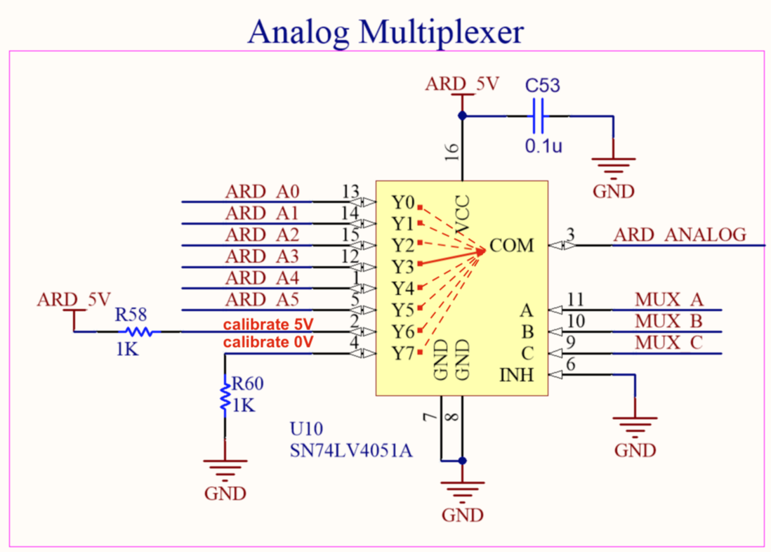
'Calibrating' the A0-A6 analog channels
As the multiplexer has 2 free inputs (Y6 and Y7), we can take advantage of this and use them to get the possibility to switch the ARD_ANALOG output to 5V and 0V. By doing this, we can compensate for the small errors added by the multiplexer and the level translator stage. The procedure could be the following:
- Select input Y6 (routed to 5V). Read the ADC output (it could be useful to take several measurements and simply average them) and store the result.
- Select input Y7 (routed to 0V). Average several ADC readings and store the result.
- Use the stored values to compensate for readings on the channels A0 to A5.
An example implementation of this procedure can be found on the [firmware ADC section].
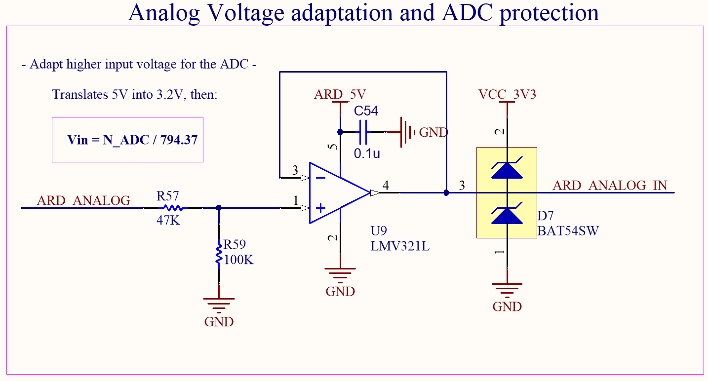
The schematic below shows the signal conditioning stage (from 5V to 3.2V) and diode clamping circuit to protect the internal ADC from voltages out of its maximum ranges.
The following table shows the combination of the multiplexer control lines needed to select each channel:
| Position | MUX_C | MUX_B | MUX_A | Channel selected |
|---|---|---|---|---|
| Y0 | 0 | 0 | 0 | A0 |
| Y1 | 0 | 0 | 1 | A1 |
| Y2 | 0 | 1 | 0 | A2 |
| Y3 | 0 | 1 | 1 | A3 |
| Y4 | 1 | 0 | 0 | A4 (1) |
| Y5 | 1 | 0 | 1 | A5 (1) |
| Y6 | 1 | 1 | 0 | Calibration High (5V) |
| Y7 | 1 | 1 | 1 | Calibration Low (0V) |
A4 and A5 inputs
In the Arduino UNO R3, and in some shields, the A4 and A5 inputs are internally connected with the I2C bus on the D15 and D14 pins (SDA and SCL lines). Therefore, in order to use the A4 and A5 pins as Analog Inputs, the correspondent I2C pins on the MCU (PB_4 and PA_8) need to be configured as high-impedance (or input, which the default state).